Atomic Layer Deposition for OLED and MicroLED Display Technologies
Fast and efficient ALD enables cost-effective encapsulation of microOLEDs and sidewall passivation of microLEDs
Display technologies have evolved rapidly over the decades, from 19” cathode ray tubes to <1um-pitched microLEDs. Consumers demand thinner screens, higher pixel densities, flexible/curved screens, and near-eye viewing distances. Organic Light Emitting Diode (OLED) displays have found success as a high performing low-cost technology in the market with a compound annual growth rate (CAGR) of 13.6% reaching $72.8 billion in 2026. MicroLEDs are a slightly newer, competitive and higher-performing technology with a CAGR of 89.3% reaching $18.8 billion by 2026. Despite the expected growth in OLED and microLED technologies, they both suffer from technical drawbacks. OLEDs suffer from short lifetimes due to moisture/oxygen infiltration and MicroLEDs struggle with scaling production due to the decreased pitch size leading to poor sidewall passivation and low pixel efficiencies. Atomic layer deposition (ALD) has the ability to improve both OLED and microLED technologies by depositing defect-free films to provide a hermetic encapsulation, and sidewall passivation to improve lifetimes.
TO LEARN MORE, DOWNLOAD THE MICRODISPLAY WHITE PAPER
ALD BENEFITS FOR MICRO DISPLAYS
Endurance
Sustained performance in harsh environments.
Light-weight
Ultra-thin film encapsulation.
Precise
100% conformal and pin hole free.
Pristine conformality in high-aspect ratio structures
Hermetic sealing encapsulation layers with minimal thickness
Ultra-low particle generation
Low stress films
Improved lifetime of OLEDs
Increased quantum efficiencies for microLEDs
ALD Improves Performance AND Lifetimes!
ALD for OLED Technology
OLEDs exhibit an attractive price-to-performance ratio but are susceptible to moisture and oxygen ingress through the organic layers within the pixel. Due to this sensitivity, OLEDs have the most stringent water vapor and oxygen transmission rate requirements of all optoelectronics technologies at 10-6 g/m2 /day and 10-3 cm3/m2 /day, respectively. Once moisture has penetrated the encapsulation surface, dark spots or “dead pixels” will appear due to the hydrolyzation of electrodes or electron injection layers.
Common VS ALD OLED Encapsulation Stack
ALD for MicroLED Technology
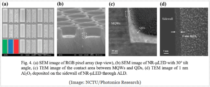
Deposition on the pixel sidewalls is an effective process to passivate the dangling bond and defects caused by the dry etching process to create the pixel trench. ALD enables passivation at ultra-high aspect ratios and outperforms PECVD passivation for EQE improvements in the same film according to a recent study with red microLED devices. Several other studies have shown ALD is the preferred passivation technique due to its excellent uniformity, high-quality film density, angstrom level thickness control and perfect surface coverage. In a 2018 study, ALD passivated sidewalls in a III-V microLED device exhibited 10% higher efficiency and conformal step coverage compared to PECVD deposited films
PECVD VS ALD Sidewall Passivation
Deposition on the pixel sidewalls is an effective process to passivate the dangling bond and defects caused by the dry etching process to create the pixel trench. ALD enables passivation at ultra-high aspect ratios and outperforms PECVD passivation for EQE improvements in the same film according to a recent study with red microLED devices. Several other studies have shown ALD is the preferred passivation technique due to its excellent uniformity, high-quality film density, angstrom level thickness control and perfect surface coverage. In a 2018 study, ALD passivated sidewalls in a III-V microLED device exhibited 10% higher efficiency and conformal step coverage compared to PECVD deposited films.

TO LEARN MORE, DOWNLOAD THE MICRODISPLAY WHITE PAPER
